http://www.sohu.com/a/278790628_610300

量子位
2533文章 0总阅读
查看TA的文章>
831
中国芯片制造迈出一大步!中科院造出最强紫外超分辨光刻机
2018-11-30 14:14 中国 /日本 /军人
问耕 乾明 郭一璞 晓查 发自 凹非寺
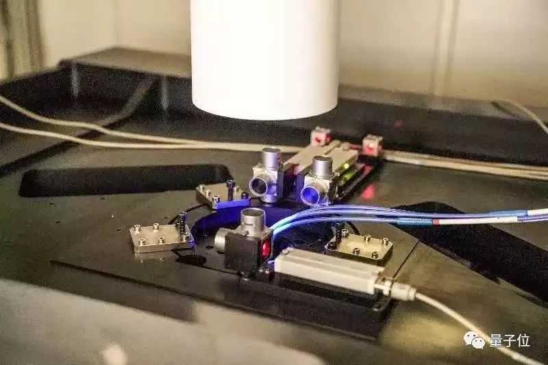
我国在芯片制造领域取得新突破!
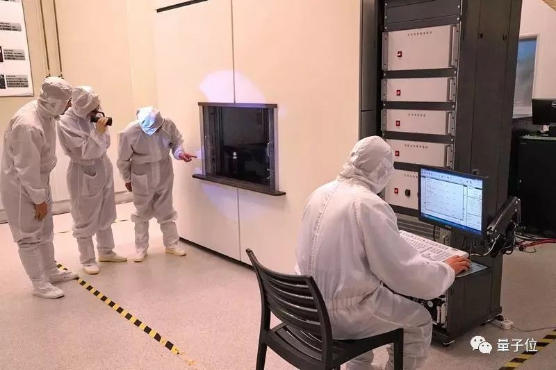
经过近七年艰苦攻关,“超分辨光刻装备研制”项目通过验收。这意味着,现在中国有了“世界上首台分辨力最高的紫外(即22纳米@365纳米)超分辨光刻装备”。
换句话说,我国科学家研制成功了一种非常强大的光刻机。
光刻机,那可是芯片制造的核心装备。我国一直在芯片行业受制于人,在光刻机领域更是如此,时常遭遇国外掐脖子、禁售等种种制约。
对于这次的突破,验收专家组的意见是:
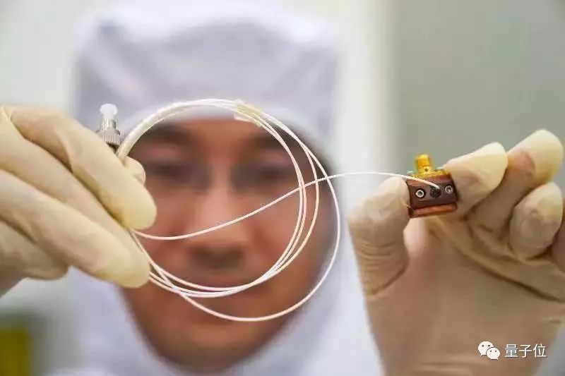
消息一出,很多人都纷纷称赞,但大多数都是不明觉厉,当然也有人说是吹牛。这个消息背后,到底意味着什么呢?
这个突破亮点很多,其中最值得关注的有几个点,量子位简单总结如下:
光源:粗刀刻细线
这个国产的光刻机,采用365纳米波长光源,属于近紫外的范围。
通常情况下,为了追求更小的纳米工艺,光刻机厂商的解决方案是,使用波长越来越短的光源。ASML就是这种思路。
现在国外使用最广泛的光刻机的光源为193纳米波长深紫外激光,光刻分辨力只有38纳米,约0.27倍曝光波长。
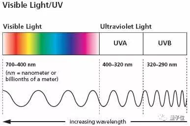
这台国产光刻机,可以做到22纳米。而且,“结合双重曝光技术后,未来还可用于制造10纳米级别的芯片”。
也就是说,中科院光电所研发的这台光刻机,用波长更长(近紫外)、成本更低(汞灯)的光源,实现了更高的光刻分辨力(0.06倍曝光波长)。
项目副总设计师、中科院光电技术研究所研究员胡松在接受《中国科学报》采访时,打了一个比方:“这相当于我们用很粗的刀,刻出一条很细的线。”这就是所谓的突破分辨力衍射极限。
因此,它也被称为世界上首台分辨力最高的紫外超分辨光刻装备。
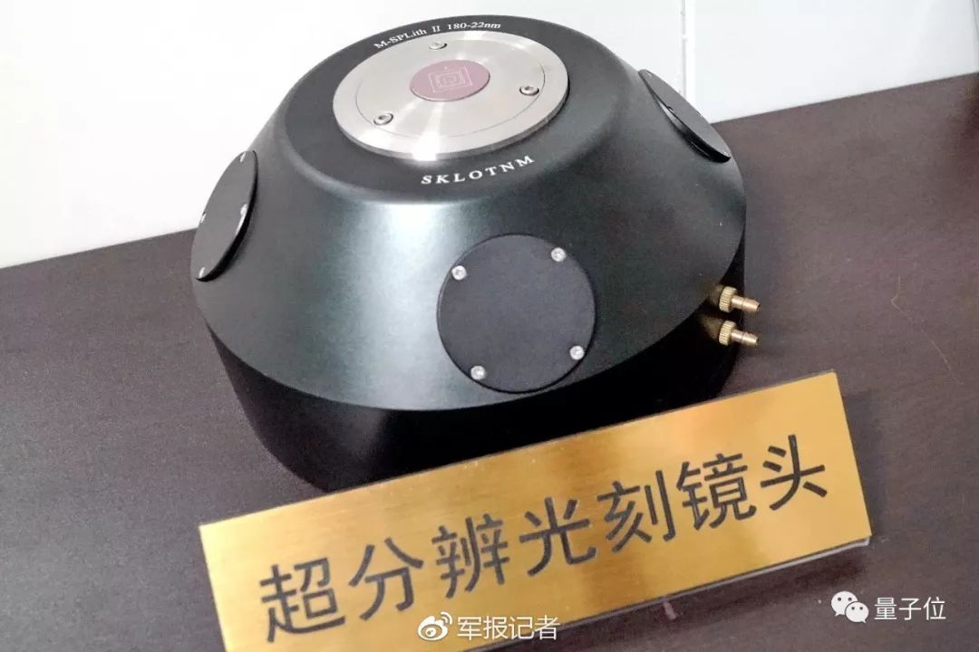
成本:高端设备“白菜价”
波长越短,成本越高。
为获得更高分辨力,传统上采用缩短光波、增加成像系统数值孔径等技术路径来改进光刻机,但问题在于不仅技术难度极高,装备成本也极高。
ASML最新的第五代光刻机使用波长更短的13.5纳米极紫外光(EUV),用于实现14纳米、10纳米、及7纳米制程的芯片生产。
一台这样的光刻机售价1亿美元以上。
而中科院光电所这台设备,使用波长更长、更普通的紫外光,意味着国产光刻机使用低成本光源,实现了更高分辨力的光刻。
有网友评价称,中国造的光刻机说不定和其他被中国攻克的高科技设备一样,以后也成了白菜价。
突破:破局禁运,弯道超车
这台光刻机的出现,还有另一个重要的意义。
这里我们引用央广的报道:
局限
当然,我们也不能头脑发热。
这个设备的出现,并不意味着我国的芯片制造立刻就能突飞猛进。一方面,芯片制造是一个庞大的产业生态,另一方面中科院光电所的光刻机还有一定的局限。
据介绍,目前这个装备已制备出一系列纳米功能器件,包括大口径薄膜镜、超导纳米线单光子探测器、切伦科夫辐射器件、生化传感芯片、超表面成像器件等,验证了该装备纳米功能器件加工能力,已达到实用化水平。
也就是说,目前主要是一些光学等领域的器件。
不过也有知乎网友表示“以目前的技术能力,只能做周期的线条和点阵,是无法制作复杂的IC需要的图形的”。
这一技术被指“在短期内是无法应用于IC制造领域的,是无法撼动ASML在IC制造领域分毫的……但形成了一定的威胁,长期还是有可能取得更重要的突破的。”
中国光刻机制造落后现状
目前国际上生产光刻机的主要厂商有荷兰的ASML、日本的尼康、佳能。其中,数ASML技术最为先进。
国内也有生产光刻机的公司,比如上海微电子装备,但技术水平远远落后于ASML。
上海微电子装备目前生产的光刻机仅能加工90纳米工艺制程芯片,这已经是国产光刻机最高水平。而ASML已经量产7纳米制程EUV光刻机,至少存在着十几年的技术差距。
光刻机是制造芯片的核心装备,过去一直是中国的技术弱项。光刻机的水平严重制约着中国芯片技术的发展。我们一直在被“卡脖子”。
国内的芯片制造商中芯国际、长江存储等厂商不得不高价从ASML买入光刻机。
今年5月,日经亚洲评论曾报道,中芯国际向国际半导体设备大厂ASML下单了一台1.2亿美元的EUV光刻机,预计将于2019年初交货。
另外,长江存储今年也从ASML买入一台浸润式光刻机,售价高达7200万美元。
那么,所谓的光刻机到底是啥?
光刻机原理
光刻机,芯片制造的核心设备之一。中科院光电所的胡松、贺晓栋在《中科院之声》发表的一篇文章中这样介绍它的重要性:
但比较特殊的是,光刻机以光为“刀具”。具体来说,工艺流程大致是这样的:
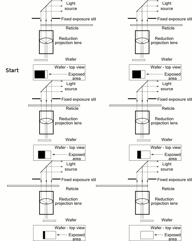
这只是一个简化的过程,通常情况下,想要用光刻机制造出一个芯片,需要在极其细微的结构上进行上百次套刻和数千道工艺,需要几百种设备才能完成。
这次中科院研制成功的光刻机,能力达到了22纳米。这是什么概念呢?中科院的文章中提到了一个对比:
这台光刻机,是谁研发出来的?
中科院光电所的7年探索
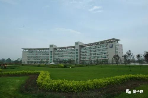
这台光刻机背后的研究机构是中科院光电所。
带头完成这项研发任务的,是中科院光电所所长、超分辨光刻装备项目首席科学家、中国科学院大学教授&博导罗先刚研究员。

罗先刚在光电领域的学术地位从他的一长串title中可见一斑:
微细加工光学技术国家重点实验室主任,国家973计划首席科学家,曾获2016年度国家技术发明一等奖,2017年中国工程院院士增选有效候选人,国家杰出青年科学基金获得者,中组部首批万人计划科技领军人才、2009年“新世纪百千万人才工程”国家级人选,2004年中科院“百人计划”入选者,中国光学学会、美国光学学会、国际光学工程学会、国际光电子与激光工程学会四大学会成员(Fellow)。
从1995年在中科院光电技术研究所读硕士开始,罗先刚已经从事光电领域20余年了,在中科院光电技术研究所读完硕士和博士后,他去了日本理化学研究所做博士后和研究科学家。
2004年,罗先刚回到了他读书的中科院光电技术研究所,开始担任研究员。20余年的光电学术之路上,他不仅发表了SCI收录论文100余篇,还带出了数十名优秀的硕士博士生。
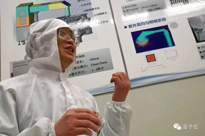
项目副总师胡松也是中科院光电技术研究所的研究员、中国科学院大学博导,在光学投影曝光微纳加工技术、 微细加工光刻技术有丰富的经验,享受国务院政府津贴,曾主持多个国家级、部委级、省级科研项目,发表十余项专利技术。
中科院光电所完成这项计划用了7年。
根据经济日报报道,2012年,中科院光电所承担了超分辨光刻装备这一国家重大科研装备项目研制任务,当时并没有任何国外成熟经验可借鉴。
7年来,项目组突破了高均匀性照明、超分辨光刻镜头、纳米级分辨力检焦及间隙测量和超精密、多自由度工件台及控制等关键技术,完成国际上首台分辨力最高的紫外超分辨光刻装备研制,其采用365纳米波长光源,单次曝光最高线宽分辨力达到22纳米(约1/17曝光波长)。
在此基础上,项目组还结合超分辨光刻装备项目开发的高深宽比刻蚀、多重图形等配套工艺,实现了10纳米以下特征尺寸图形的加工。
另外,这个项目还发表了论文68篇,申请国家发明专利92项,其中授权47项,申请国际专利8项,授权4项,为国家培养了一支超分辨光刻技术和装备研发团队。
— 完—返回搜狐,查看更多
声明:该文观点仅代表作者本人,搜狐号系信息发布平台,搜狐仅提供信息存储空间服务。
Qubit
2533 articles
0 total reading
View TA's article >
831
share to
China's chip manufacturing has taken a big step! The Chinese Academy of Sciences has produced the strongest UV super-resolution lithography machine
2018-11-30 14:14
China
/
Japan
/
soldier
Qong Geng Qian Ming Guo Yizhen Xiaocha from the concave temple
China has made new breakthroughs in the field of chip manufacturing!
After nearly seven years of hard work, the "Super Resolution Lithography Equipment Development" project passed the acceptance test. This means that China now has the world's first high-resolution UV (ie 22 nm @ 365 nm) super-resolution lithography equipment.
In other words, Chinese scientists have developed a very powerful lithography machine.
The lithography machine, that is the core equipment for chip manufacturing. China has always been subject to people in the chip industry, especially in the field of lithography machines, and often encounters various restrictions such as foreign neck and ban.
For this breakthrough, the acceptance panel’s comments are:
The lithography machine has a maximum linewidth resolution of 22 nm in a single exposure at a wavelength of 365 nm. In principle, the project breaks through the resolution diffraction limit and establishes a new high-resolution, large-area nanolithography equipment research and development route to bypass foreign intellectual property barriers.
When the news came out, many people praised it, but most of them were unconscious. Of course, some people said that it was bragging. What does it mean behind this news?
There are many highlights in this breakthrough. Among them, there are several points that are most worthy of attention. The qubits are briefly summarized as follows:
Light source: coarse knife engraved thin line
This domestic lithography machine uses a 365 nm wavelength source, which belongs to the near-ultraviolet range.
In general, in order to pursue smaller nano-processes, the lithography machine manufacturer's solution is to use light sources with shorter and shorter wavelengths. ASML is the way of thinking.
The light source of the most widely used lithography machine in foreign countries is a 193 nm wavelength deep ultraviolet laser with a lithography resolution of only 38 nm and an exposure wavelength of about 0.27.
This domestic lithography machine can achieve 22 nanometers. Moreover, "in combination with the double exposure technology, the future can also be used to manufacture chips of the 10 nanometer level."
That is to say, the lithography machine developed by the Institute of Optoelectronics of the Chinese Academy of Sciences uses a light source with a longer wavelength (near-ultraviolet) and a lower cost (mercury lamp) to achieve higher lithography resolution (0.06 times exposure wavelength).
Hu Song, deputy chief designer of the project and researcher of the Institute of Optoelectronic Technology of the Chinese Academy of Sciences, made an analogy in an interview with the Journal of the Chinese Academy of Sciences: "This is equivalent to using a very thick knife to engrave a very thin line." It is the so-called breakthrough resolution diffraction limit.
Therefore, it is also known as the world's first high-resolution UV super-resolution lithography equipment.
Cost: high-end equipment "cabbage price"
The shorter the wavelength, the higher the cost.
In order to obtain higher resolution, the lithography machine has been traditionally improved by shortening the light wave and increasing the numerical aperture of the imaging system, but the problem is that the technical difficulty is extremely high and the equipment cost is also extremely high.
ASML's latest fifth-generation lithography machine uses a shorter wavelength of 13.5 nanometer extreme ultraviolet (EUV) for chip production at 14nm, 10nm, and 7nm processes.
One such lithography machine is priced at more than $100 million.
The equipment of the Institute of Optoelectronics of the Chinese Academy of Sciences uses longer wavelength and more common ultraviolet light, which means that domestic lithography machines use low-cost light sources to achieve higher resolution lithography.
Some netizens commented that the Chinese-made lithography machine may be the same as other high-tech equipment that was conquered by China.
Breakthrough: breaking the embargo, overtaking the corner
The emergence of this lithography machine has another important significance.
Here we quote the report of Yangguang:
The smooth implementation of the super-resolution lithography equipment project has broken the monopoly of foreign high-end lithography equipment, providing a new solution for nano-optical processing, as well as advanced strategic technology fields such as new generation information technology, new materials, and biomedical technology. The core frontier and defense security provide core technical support.
Hu Song, deputy chief designer of the project and researcher of the Institute of Optoelectronic Technology of the Chinese Academy of Sciences, said: "The first one is first manifested at our current level and internationally, and can reach a consistent level. The resolution index is actually a foreign embargo. An indicator, after our project came out, will be of great help in breaking the embargo."
"The second one is not to be afraid if it is embargoed abroad. Because our technology goes on, we think it can be guaranteed. In the future development of chips, the next generation of opto-mechatronics chips or the generalized chips we are talking about (development areas), Maybe the corner road is overtaking."
Limit
Of course, we can't be too hot.
The emergence of this equipment does not mean that China's chip manufacturing will be able to make rapid progress immediately. On the one hand, chip manufacturing is a huge industrial ecology. On the other hand, the lithography machine of the Institute of Optoelectronics of the Chinese Academy of Sciences has certain limitations.
According to reports, the current equipment has prepared a series of nano-functional devices, including large-diameter thin film mirrors, superconducting nanowire single photon detectors, Cherenkov radiation devices, biochemical sensor chips, super-surface imaging devices, etc., verified The processing capability of the nano-functional device has reached a practical level.
That is to say, at present, it is mainly some devices in the field of optics and the like.
However, some netizens said that "with current technical capabilities, only periodic lines and lattices can be used to create complex ICs."
This technology is said to be "in the short-term, it can not be applied to the field of IC manufacturing, it is impossible to shake ASML in the field of IC manufacturing ... but it has formed a certain threat, and it is still possible to achieve more important breakthroughs in the long run."
China's lithography machine manufacturing backward status
At present, the main manufacturers of lithography machines in the world are ASML in the Netherlands, Nikon in Japan, and Canon. Among them, the number of ASML technology is the most advanced.
There are also companies producing lithography machines in China, such as Shanghai microelectronics equipment, but the technical level is far behind ASML.
The lithography machine currently produced by Shanghai Microelectronics Equipment can only process 90nm process chip, which is the highest level of domestic lithography machine. ASML has already mass-produced 7-nanometer EUV lithography machines, at least for more than a decade.
The lithography machine is the core equipment for manufacturing chips, and it has always been a technical weakness in China. The level of lithography machine seriously restricts the development of China's chip technology. We have been "card neck".
Domestic chip makers such as SMIC and Changjiang Storage have to buy lithography machines from ASML at a high price.
In May of this year, the Nikkei Asian Review reported that SMIC had placed a $120 million EUV lithography machine at ASML, an international semiconductor equipment manufacturer, which is expected to be delivered in early 2019.
In addition, Changjiang Storage also bought an infiltration lithography machine from ASML this year, priced at up to $ 72 million.
So, what is the so-called lithography machine?
Lithography principle
A lithography machine, one of the core devices for chip manufacturing. Hu Song and He Xiaodong of the Institute of Optoelectronics of the Chinese Academy of Sciences introduced the importance of this in an article published in The Voice of the Chinese Academy of Sciences:
The post-industrial era, including the current industry 3.0 and industry 4.0, is based on chips. As a tool for manufacturing chips, the lithography machine is equivalent to the machine tools of the industrial age and the hands of the pre-industrial era.
But what is special is that the lithography machine uses light as a "tool." Specifically, the process flow is roughly like this:
The surface of the silicon wafer is covered with a highly photosensitive photoresist, and then the light is transmitted through the mask to the surface of the silicon wafer, and the photoresist irradiated by the light reacts.
Thereafter, the irradiated/unirradiated photoresist is washed away with a specific solvent to effect transfer of the circuit pattern from the mask to the silicon wafer.
Quoted from: "A text to understand the lithography machine", Huachuang Securities
This is just a simplification process. Usually, if you want to use a lithography machine to make a chip, you need to perform hundreds of engravings and thousands of processes on extremely fine structures, which require hundreds of devices.
The lithography machine successfully developed by the Chinese Academy of Sciences has a capacity of 22 nanometers. what is this concept? A comparison is mentioned in the article of the Chinese Academy of Sciences:
The hair has a diameter of about 80 microns and 22 nanometers is 1/3600 of the hair diameter. That is to say, this lithography machine is capable of processing various complicated structures on the surface of the hair.
Who developed this lithography machine?
7 years of exploration by the Institute of Optoelectronics, Chinese Academy of Sciences
The research institute behind this lithography machine is the Institute of Optoelectronics of the Chinese Academy of Sciences.
Leading the research and development task is the director of the Institute of Optoelectronics of the Chinese Academy of Sciences, the chief scientist of the super-resolution lithography equipment project, and the professor of the Chinese Academy of Sciences & Professor Luo Xiangang.
Luo Xiangang's academic status in the field of optoelectronics can be seen in his long list of titles:
Director of State Key Laboratory of Microfabrication Optics, Chief Scientist of National 973 Program, won the first prize of 2016 National Technology Invention, 2017 Chinese Academy of Engineering academician co-opted effective candidate, National Outstanding Youth Science Fund winner, middle group leader The 10,000-person plan for science and technology leading talents, the 2009 National Talents of the "New Century Talents Project", the winners of the "Hundred Talents Program" of the Chinese Academy of Sciences in 2004, the Chinese Optical Society, the Optical Society of America, the International Society of Optical Engineering, the International Optoelectronics and Lasers Member of the Four Engineering Association of the Engineering Society (Fellow).
Since he started his master's degree at the Institute of Optoelectronic Technology of the Chinese Academy of Sciences in 1995, Luo Xiangang has been engaged in the field of optoelectronics for more than 20 years. After completing his master's and postdoctoral degrees at the Institute of Optoelectronic Technology of the Chinese Academy of Sciences, he went to postdoctoral and research scientists in Japanese physiochemical research.
In 2004, Luo Xiangang returned to the Institute of Optoelectronic Technology of the Chinese Academy of Sciences and began to work as a researcher. On the road of optoelectronics for more than 20 years, he not only published more than 100 papers in SCI, but also brought out dozens of outstanding master's and doctoral students.
Hu Song, deputy director of the project, is also a researcher at the Institute of Optoelectronic Technology of the Chinese Academy of Sciences and a doctoral supervisor at the University of Chinese Academy of Sciences. He has extensive experience in optical projection exposure micro-nano processing technology and micro-machining lithography technology. He enjoys government subsidies from the State Council and has presided over several national standards. At the ministerial level and provincial level scientific research projects, more than ten patent technologies were published.
It took seven years for the Institute of Optoelectronics of the Chinese Academy of Sciences to complete this project.
According to the Economic Daily, in 2012, the Institute of Optoelectronics of the Chinese Academy of Sciences undertook the task of developing a national research equipment project for super-resolution lithography equipment. At that time, there was no foreign mature experience to draw on.
In the past 7 years, the project team has broken through the key technologies of high uniformity illumination, super-resolution lithography lens, nano-resolution resolution and gap measurement and ultra-precision, multi-degree-of-freedom workpiece table and control, achieving the highest resolution in the world. The UV super-resolution lithography equipment was developed using a 365 nm wavelength source with a maximum linewidth resolution of 22 nm (approximately 1/17 exposure wavelength) in a single exposure.
On this basis, the project team also combined the high-aspect ratio etching and multi-patterning technology developed by the super-resolution lithography equipment project to realize the processing of feature size graphics below 10 nm.
In addition, this project also published 68 papers, applied for 92 national invention patents, including 47 authorizations, 8 international patents, 4 authorizations, and trained a super-resolution lithography technology and equipment R&D team for the country.
— End — Return to Sohu, see more
Disclaimer: This article only represents the author himself, Sohu is the information publishing platform, and Sohu only provides information storage space services.
量子位
2533文章 0总阅读
查看TA的文章>
831
- 分享到
中国芯片制造迈出一大步!中科院造出最强紫外超分辨光刻机
2018-11-30 14:14 中国 /日本 /军人
问耕 乾明 郭一璞 晓查 发自 凹非寺

我国在芯片制造领域取得新突破!
经过近七年艰苦攻关,“超分辨光刻装备研制”项目通过验收。这意味着,现在中国有了“世界上首台分辨力最高的紫外(即22纳米@365纳米)超分辨光刻装备”。
换句话说,我国科学家研制成功了一种非常强大的光刻机。
光刻机,那可是芯片制造的核心装备。我国一直在芯片行业受制于人,在光刻机领域更是如此,时常遭遇国外掐脖子、禁售等种种制约。
对于这次的突破,验收专家组的意见是:
该光刻机在365纳米光源波长下,单次曝光最高线宽分辨力达到22纳米。项目在原理上突破分辨力衍射极限,建立了一条高分辨、大面积的纳米光刻装备研发新路线,绕过国外相关知识产权壁垒。

消息一出,很多人都纷纷称赞,但大多数都是不明觉厉,当然也有人说是吹牛。这个消息背后,到底意味着什么呢?
这个突破亮点很多,其中最值得关注的有几个点,量子位简单总结如下:
光源:粗刀刻细线
这个国产的光刻机,采用365纳米波长光源,属于近紫外的范围。
通常情况下,为了追求更小的纳米工艺,光刻机厂商的解决方案是,使用波长越来越短的光源。ASML就是这种思路。
现在国外使用最广泛的光刻机的光源为193纳米波长深紫外激光,光刻分辨力只有38纳米,约0.27倍曝光波长。

这台国产光刻机,可以做到22纳米。而且,“结合双重曝光技术后,未来还可用于制造10纳米级别的芯片”。
也就是说,中科院光电所研发的这台光刻机,用波长更长(近紫外)、成本更低(汞灯)的光源,实现了更高的光刻分辨力(0.06倍曝光波长)。
项目副总设计师、中科院光电技术研究所研究员胡松在接受《中国科学报》采访时,打了一个比方:“这相当于我们用很粗的刀,刻出一条很细的线。”这就是所谓的突破分辨力衍射极限。
因此,它也被称为世界上首台分辨力最高的紫外超分辨光刻装备。

成本:高端设备“白菜价”
波长越短,成本越高。
为获得更高分辨力,传统上采用缩短光波、增加成像系统数值孔径等技术路径来改进光刻机,但问题在于不仅技术难度极高,装备成本也极高。
ASML最新的第五代光刻机使用波长更短的13.5纳米极紫外光(EUV),用于实现14纳米、10纳米、及7纳米制程的芯片生产。
一台这样的光刻机售价1亿美元以上。
而中科院光电所这台设备,使用波长更长、更普通的紫外光,意味着国产光刻机使用低成本光源,实现了更高分辨力的光刻。
有网友评价称,中国造的光刻机说不定和其他被中国攻克的高科技设备一样,以后也成了白菜价。

突破:破局禁运,弯道超车
这台光刻机的出现,还有另一个重要的意义。
这里我们引用央广的报道:
超分辨光刻装备项目的顺利实施,打破了国外在高端光刻装备领域的垄断,为纳米光学加工提供了全新的解决途径,也为新一代信息技术、新材料、生物医疗等先进战略技术领域,基础前沿和国防安全提供了核心技术保障。
项目副总设计师、中科院光电技术研究所研究员胡松介绍:“第一个首先表现于我们现在的水平和国际上已经可以达到持一致的水平。分辨率的指标实际上也是属于国外禁运的一个指标,我们这项目出来之后对打破禁运有很大的帮助。”
“第二个如果国外禁运我们也不用怕,因为我们这个技术再走下去,我们认为可以有保证。在芯片未来发展、下一代光机电集成芯片或者我们说的广义芯片(研制领域),有可能弯道超车走在更前面。”
项目副总设计师、中科院光电技术研究所研究员胡松介绍:“第一个首先表现于我们现在的水平和国际上已经可以达到持一致的水平。分辨率的指标实际上也是属于国外禁运的一个指标,我们这项目出来之后对打破禁运有很大的帮助。”
“第二个如果国外禁运我们也不用怕,因为我们这个技术再走下去,我们认为可以有保证。在芯片未来发展、下一代光机电集成芯片或者我们说的广义芯片(研制领域),有可能弯道超车走在更前面。”

局限
当然,我们也不能头脑发热。
这个设备的出现,并不意味着我国的芯片制造立刻就能突飞猛进。一方面,芯片制造是一个庞大的产业生态,另一方面中科院光电所的光刻机还有一定的局限。
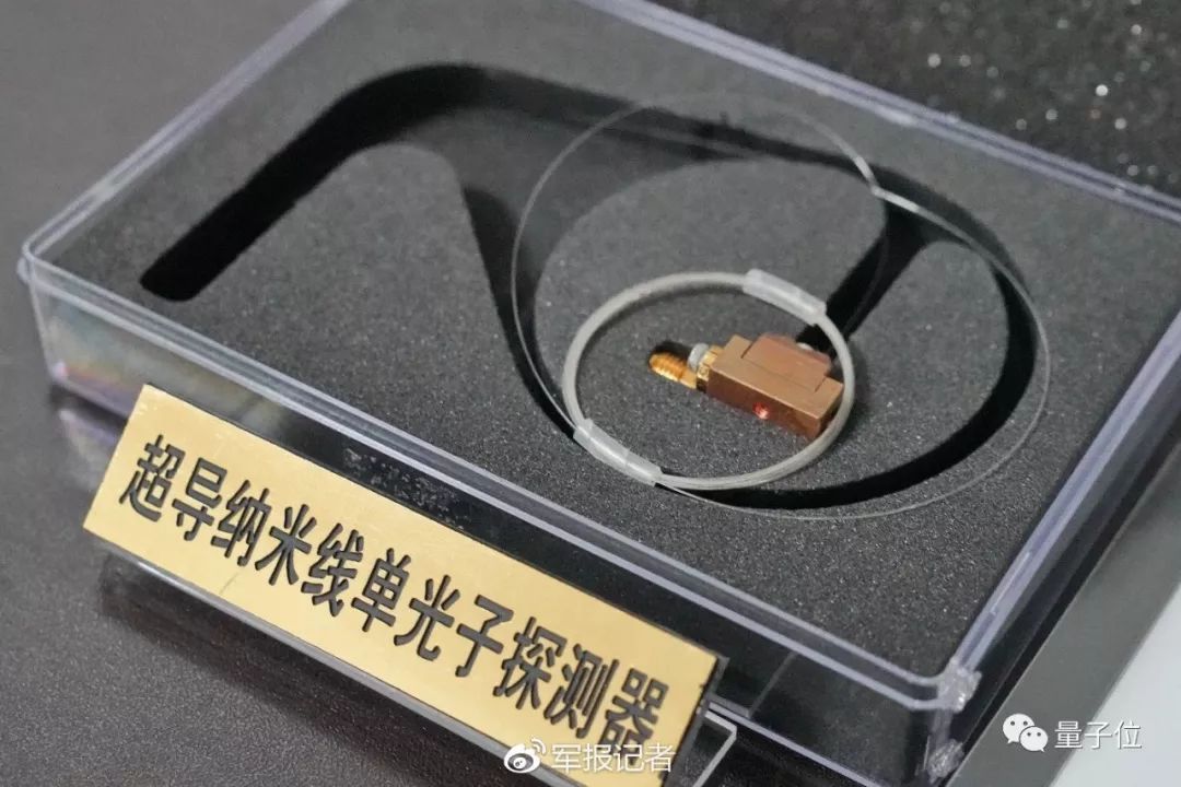
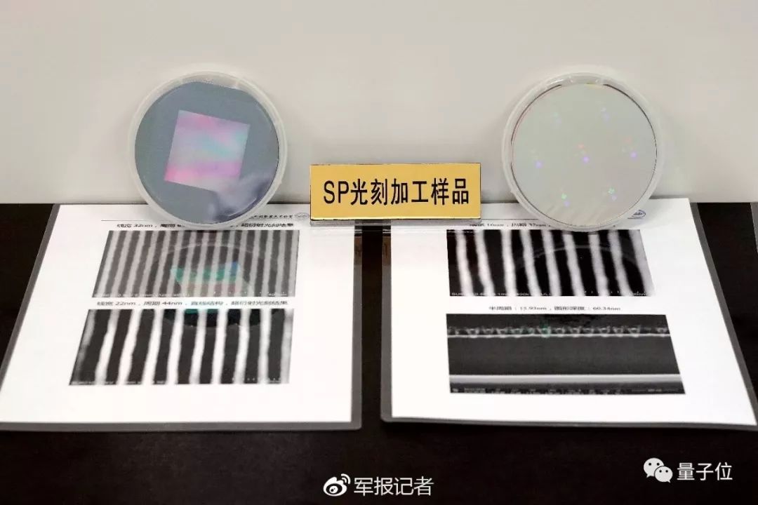
据介绍,目前这个装备已制备出一系列纳米功能器件,包括大口径薄膜镜、超导纳米线单光子探测器、切伦科夫辐射器件、生化传感芯片、超表面成像器件等,验证了该装备纳米功能器件加工能力,已达到实用化水平。

也就是说,目前主要是一些光学等领域的器件。
不过也有知乎网友表示“以目前的技术能力,只能做周期的线条和点阵,是无法制作复杂的IC需要的图形的”。
这一技术被指“在短期内是无法应用于IC制造领域的,是无法撼动ASML在IC制造领域分毫的……但形成了一定的威胁,长期还是有可能取得更重要的突破的。”
中国光刻机制造落后现状
目前国际上生产光刻机的主要厂商有荷兰的ASML、日本的尼康、佳能。其中,数ASML技术最为先进。
国内也有生产光刻机的公司,比如上海微电子装备,但技术水平远远落后于ASML。
上海微电子装备目前生产的光刻机仅能加工90纳米工艺制程芯片,这已经是国产光刻机最高水平。而ASML已经量产7纳米制程EUV光刻机,至少存在着十几年的技术差距。
光刻机是制造芯片的核心装备,过去一直是中国的技术弱项。光刻机的水平严重制约着中国芯片技术的发展。我们一直在被“卡脖子”。
国内的芯片制造商中芯国际、长江存储等厂商不得不高价从ASML买入光刻机。

今年5月,日经亚洲评论曾报道,中芯国际向国际半导体设备大厂ASML下单了一台1.2亿美元的EUV光刻机,预计将于2019年初交货。
另外,长江存储今年也从ASML买入一台浸润式光刻机,售价高达7200万美元。
那么,所谓的光刻机到底是啥?
光刻机原理
光刻机,芯片制造的核心设备之一。中科院光电所的胡松、贺晓栋在《中科院之声》发表的一篇文章中这样介绍它的重要性:
后工业时代包括现在的工业3.0、工业4.0,都以芯片为基础,光刻机作为制造芯片的工具,就相当于工业时代的机床,前工业时代的人手。
但比较特殊的是,光刻机以光为“刀具”。具体来说,工艺流程大致是这样的:
在硅片表面覆盖一层具有高度光敏感性光刻胶,再用光线透过掩模照射在硅片表面,被光线照射到的光刻胶会发生反应。
此后用特定溶剂洗去被照射/未被照射的光刻胶, 就实现了电路图从掩模到硅片的转移。
引自:《一文看懂光刻机》,华创证券
此后用特定溶剂洗去被照射/未被照射的光刻胶, 就实现了电路图从掩模到硅片的转移。
引自:《一文看懂光刻机》,华创证券

这只是一个简化的过程,通常情况下,想要用光刻机制造出一个芯片,需要在极其细微的结构上进行上百次套刻和数千道工艺,需要几百种设备才能完成。
这次中科院研制成功的光刻机,能力达到了22纳米。这是什么概念呢?中科院的文章中提到了一个对比:
头发的直径约为80微米,22纳米是头发直径的1/3600。也就是说,这个光刻机能够在头发表面加工各种复杂的结构。
这台光刻机,是谁研发出来的?
中科院光电所的7年探索

这台光刻机背后的研究机构是中科院光电所。
带头完成这项研发任务的,是中科院光电所所长、超分辨光刻装备项目首席科学家、中国科学院大学教授&博导罗先刚研究员。

罗先刚在光电领域的学术地位从他的一长串title中可见一斑:
微细加工光学技术国家重点实验室主任,国家973计划首席科学家,曾获2016年度国家技术发明一等奖,2017年中国工程院院士增选有效候选人,国家杰出青年科学基金获得者,中组部首批万人计划科技领军人才、2009年“新世纪百千万人才工程”国家级人选,2004年中科院“百人计划”入选者,中国光学学会、美国光学学会、国际光学工程学会、国际光电子与激光工程学会四大学会成员(Fellow)。
从1995年在中科院光电技术研究所读硕士开始,罗先刚已经从事光电领域20余年了,在中科院光电技术研究所读完硕士和博士后,他去了日本理化学研究所做博士后和研究科学家。
2004年,罗先刚回到了他读书的中科院光电技术研究所,开始担任研究员。20余年的光电学术之路上,他不仅发表了SCI收录论文100余篇,还带出了数十名优秀的硕士博士生。

项目副总师胡松也是中科院光电技术研究所的研究员、中国科学院大学博导,在光学投影曝光微纳加工技术、 微细加工光刻技术有丰富的经验,享受国务院政府津贴,曾主持多个国家级、部委级、省级科研项目,发表十余项专利技术。
中科院光电所完成这项计划用了7年。
根据经济日报报道,2012年,中科院光电所承担了超分辨光刻装备这一国家重大科研装备项目研制任务,当时并没有任何国外成熟经验可借鉴。
7年来,项目组突破了高均匀性照明、超分辨光刻镜头、纳米级分辨力检焦及间隙测量和超精密、多自由度工件台及控制等关键技术,完成国际上首台分辨力最高的紫外超分辨光刻装备研制,其采用365纳米波长光源,单次曝光最高线宽分辨力达到22纳米(约1/17曝光波长)。
在此基础上,项目组还结合超分辨光刻装备项目开发的高深宽比刻蚀、多重图形等配套工艺,实现了10纳米以下特征尺寸图形的加工。
另外,这个项目还发表了论文68篇,申请国家发明专利92项,其中授权47项,申请国际专利8项,授权4项,为国家培养了一支超分辨光刻技术和装备研发团队。
— 完—返回搜狐,查看更多
声明:该文观点仅代表作者本人,搜狐号系信息发布平台,搜狐仅提供信息存储空间服务。
Qubit
2533 articles
0 total reading
View TA's article >
831
share to
China's chip manufacturing has taken a big step! The Chinese Academy of Sciences has produced the strongest UV super-resolution lithography machine
2018-11-30 14:14
China
/
Japan
/
soldier
Qong Geng Qian Ming Guo Yizhen Xiaocha from the concave temple
China has made new breakthroughs in the field of chip manufacturing!
After nearly seven years of hard work, the "Super Resolution Lithography Equipment Development" project passed the acceptance test. This means that China now has the world's first high-resolution UV (ie 22 nm @ 365 nm) super-resolution lithography equipment.
In other words, Chinese scientists have developed a very powerful lithography machine.
The lithography machine, that is the core equipment for chip manufacturing. China has always been subject to people in the chip industry, especially in the field of lithography machines, and often encounters various restrictions such as foreign neck and ban.
For this breakthrough, the acceptance panel’s comments are:
The lithography machine has a maximum linewidth resolution of 22 nm in a single exposure at a wavelength of 365 nm. In principle, the project breaks through the resolution diffraction limit and establishes a new high-resolution, large-area nanolithography equipment research and development route to bypass foreign intellectual property barriers.
When the news came out, many people praised it, but most of them were unconscious. Of course, some people said that it was bragging. What does it mean behind this news?
There are many highlights in this breakthrough. Among them, there are several points that are most worthy of attention. The qubits are briefly summarized as follows:
Light source: coarse knife engraved thin line
This domestic lithography machine uses a 365 nm wavelength source, which belongs to the near-ultraviolet range.
In general, in order to pursue smaller nano-processes, the lithography machine manufacturer's solution is to use light sources with shorter and shorter wavelengths. ASML is the way of thinking.
The light source of the most widely used lithography machine in foreign countries is a 193 nm wavelength deep ultraviolet laser with a lithography resolution of only 38 nm and an exposure wavelength of about 0.27.
This domestic lithography machine can achieve 22 nanometers. Moreover, "in combination with the double exposure technology, the future can also be used to manufacture chips of the 10 nanometer level."
That is to say, the lithography machine developed by the Institute of Optoelectronics of the Chinese Academy of Sciences uses a light source with a longer wavelength (near-ultraviolet) and a lower cost (mercury lamp) to achieve higher lithography resolution (0.06 times exposure wavelength).
Hu Song, deputy chief designer of the project and researcher of the Institute of Optoelectronic Technology of the Chinese Academy of Sciences, made an analogy in an interview with the Journal of the Chinese Academy of Sciences: "This is equivalent to using a very thick knife to engrave a very thin line." It is the so-called breakthrough resolution diffraction limit.
Therefore, it is also known as the world's first high-resolution UV super-resolution lithography equipment.
Cost: high-end equipment "cabbage price"
The shorter the wavelength, the higher the cost.
In order to obtain higher resolution, the lithography machine has been traditionally improved by shortening the light wave and increasing the numerical aperture of the imaging system, but the problem is that the technical difficulty is extremely high and the equipment cost is also extremely high.
ASML's latest fifth-generation lithography machine uses a shorter wavelength of 13.5 nanometer extreme ultraviolet (EUV) for chip production at 14nm, 10nm, and 7nm processes.
One such lithography machine is priced at more than $100 million.
The equipment of the Institute of Optoelectronics of the Chinese Academy of Sciences uses longer wavelength and more common ultraviolet light, which means that domestic lithography machines use low-cost light sources to achieve higher resolution lithography.
Some netizens commented that the Chinese-made lithography machine may be the same as other high-tech equipment that was conquered by China.
Breakthrough: breaking the embargo, overtaking the corner
The emergence of this lithography machine has another important significance.
Here we quote the report of Yangguang:
The smooth implementation of the super-resolution lithography equipment project has broken the monopoly of foreign high-end lithography equipment, providing a new solution for nano-optical processing, as well as advanced strategic technology fields such as new generation information technology, new materials, and biomedical technology. The core frontier and defense security provide core technical support.
Hu Song, deputy chief designer of the project and researcher of the Institute of Optoelectronic Technology of the Chinese Academy of Sciences, said: "The first one is first manifested at our current level and internationally, and can reach a consistent level. The resolution index is actually a foreign embargo. An indicator, after our project came out, will be of great help in breaking the embargo."
"The second one is not to be afraid if it is embargoed abroad. Because our technology goes on, we think it can be guaranteed. In the future development of chips, the next generation of opto-mechatronics chips or the generalized chips we are talking about (development areas), Maybe the corner road is overtaking."
Limit
Of course, we can't be too hot.
The emergence of this equipment does not mean that China's chip manufacturing will be able to make rapid progress immediately. On the one hand, chip manufacturing is a huge industrial ecology. On the other hand, the lithography machine of the Institute of Optoelectronics of the Chinese Academy of Sciences has certain limitations.
According to reports, the current equipment has prepared a series of nano-functional devices, including large-diameter thin film mirrors, superconducting nanowire single photon detectors, Cherenkov radiation devices, biochemical sensor chips, super-surface imaging devices, etc., verified The processing capability of the nano-functional device has reached a practical level.
That is to say, at present, it is mainly some devices in the field of optics and the like.
However, some netizens said that "with current technical capabilities, only periodic lines and lattices can be used to create complex ICs."
This technology is said to be "in the short-term, it can not be applied to the field of IC manufacturing, it is impossible to shake ASML in the field of IC manufacturing ... but it has formed a certain threat, and it is still possible to achieve more important breakthroughs in the long run."
China's lithography machine manufacturing backward status
At present, the main manufacturers of lithography machines in the world are ASML in the Netherlands, Nikon in Japan, and Canon. Among them, the number of ASML technology is the most advanced.
There are also companies producing lithography machines in China, such as Shanghai microelectronics equipment, but the technical level is far behind ASML.
The lithography machine currently produced by Shanghai Microelectronics Equipment can only process 90nm process chip, which is the highest level of domestic lithography machine. ASML has already mass-produced 7-nanometer EUV lithography machines, at least for more than a decade.
The lithography machine is the core equipment for manufacturing chips, and it has always been a technical weakness in China. The level of lithography machine seriously restricts the development of China's chip technology. We have been "card neck".
Domestic chip makers such as SMIC and Changjiang Storage have to buy lithography machines from ASML at a high price.
In May of this year, the Nikkei Asian Review reported that SMIC had placed a $120 million EUV lithography machine at ASML, an international semiconductor equipment manufacturer, which is expected to be delivered in early 2019.
In addition, Changjiang Storage also bought an infiltration lithography machine from ASML this year, priced at up to $ 72 million.
So, what is the so-called lithography machine?
Lithography principle
A lithography machine, one of the core devices for chip manufacturing. Hu Song and He Xiaodong of the Institute of Optoelectronics of the Chinese Academy of Sciences introduced the importance of this in an article published in The Voice of the Chinese Academy of Sciences:
The post-industrial era, including the current industry 3.0 and industry 4.0, is based on chips. As a tool for manufacturing chips, the lithography machine is equivalent to the machine tools of the industrial age and the hands of the pre-industrial era.
But what is special is that the lithography machine uses light as a "tool." Specifically, the process flow is roughly like this:
The surface of the silicon wafer is covered with a highly photosensitive photoresist, and then the light is transmitted through the mask to the surface of the silicon wafer, and the photoresist irradiated by the light reacts.
Thereafter, the irradiated/unirradiated photoresist is washed away with a specific solvent to effect transfer of the circuit pattern from the mask to the silicon wafer.
Quoted from: "A text to understand the lithography machine", Huachuang Securities
This is just a simplification process. Usually, if you want to use a lithography machine to make a chip, you need to perform hundreds of engravings and thousands of processes on extremely fine structures, which require hundreds of devices.
The lithography machine successfully developed by the Chinese Academy of Sciences has a capacity of 22 nanometers. what is this concept? A comparison is mentioned in the article of the Chinese Academy of Sciences:
The hair has a diameter of about 80 microns and 22 nanometers is 1/3600 of the hair diameter. That is to say, this lithography machine is capable of processing various complicated structures on the surface of the hair.
Who developed this lithography machine?
7 years of exploration by the Institute of Optoelectronics, Chinese Academy of Sciences
The research institute behind this lithography machine is the Institute of Optoelectronics of the Chinese Academy of Sciences.
Leading the research and development task is the director of the Institute of Optoelectronics of the Chinese Academy of Sciences, the chief scientist of the super-resolution lithography equipment project, and the professor of the Chinese Academy of Sciences & Professor Luo Xiangang.
Luo Xiangang's academic status in the field of optoelectronics can be seen in his long list of titles:
Director of State Key Laboratory of Microfabrication Optics, Chief Scientist of National 973 Program, won the first prize of 2016 National Technology Invention, 2017 Chinese Academy of Engineering academician co-opted effective candidate, National Outstanding Youth Science Fund winner, middle group leader The 10,000-person plan for science and technology leading talents, the 2009 National Talents of the "New Century Talents Project", the winners of the "Hundred Talents Program" of the Chinese Academy of Sciences in 2004, the Chinese Optical Society, the Optical Society of America, the International Society of Optical Engineering, the International Optoelectronics and Lasers Member of the Four Engineering Association of the Engineering Society (Fellow).
Since he started his master's degree at the Institute of Optoelectronic Technology of the Chinese Academy of Sciences in 1995, Luo Xiangang has been engaged in the field of optoelectronics for more than 20 years. After completing his master's and postdoctoral degrees at the Institute of Optoelectronic Technology of the Chinese Academy of Sciences, he went to postdoctoral and research scientists in Japanese physiochemical research.
In 2004, Luo Xiangang returned to the Institute of Optoelectronic Technology of the Chinese Academy of Sciences and began to work as a researcher. On the road of optoelectronics for more than 20 years, he not only published more than 100 papers in SCI, but also brought out dozens of outstanding master's and doctoral students.
Hu Song, deputy director of the project, is also a researcher at the Institute of Optoelectronic Technology of the Chinese Academy of Sciences and a doctoral supervisor at the University of Chinese Academy of Sciences. He has extensive experience in optical projection exposure micro-nano processing technology and micro-machining lithography technology. He enjoys government subsidies from the State Council and has presided over several national standards. At the ministerial level and provincial level scientific research projects, more than ten patent technologies were published.
It took seven years for the Institute of Optoelectronics of the Chinese Academy of Sciences to complete this project.
According to the Economic Daily, in 2012, the Institute of Optoelectronics of the Chinese Academy of Sciences undertook the task of developing a national research equipment project for super-resolution lithography equipment. At that time, there was no foreign mature experience to draw on.
In the past 7 years, the project team has broken through the key technologies of high uniformity illumination, super-resolution lithography lens, nano-resolution resolution and gap measurement and ultra-precision, multi-degree-of-freedom workpiece table and control, achieving the highest resolution in the world. The UV super-resolution lithography equipment was developed using a 365 nm wavelength source with a maximum linewidth resolution of 22 nm (approximately 1/17 exposure wavelength) in a single exposure.
On this basis, the project team also combined the high-aspect ratio etching and multi-patterning technology developed by the super-resolution lithography equipment project to realize the processing of feature size graphics below 10 nm.
In addition, this project also published 68 papers, applied for 92 national invention patents, including 47 authorizations, 8 international patents, 4 authorizations, and trained a super-resolution lithography technology and equipment R&D team for the country.
— End — Return to Sohu, see more
Disclaimer: This article only represents the author himself, Sohu is the information publishing platform, and Sohu only provides information storage space services.

